The full form of BARITT Diode is BARrier Injection Transit Time diode. These are the latest invention in this family. Though these diodes have long drift regions like IMPATT diodes, the carrier injection in BARITT diodes is caused by forward biased junctions, but not from the plasma of an avalanche region as in them.
In IMPATT diodes, the carrier injection is quite noisy due to the impact ionization. In BARITT diodes, to avoid the noise, carrier injection is provided by punch through of the depletion region. The negative resistance in a BARITT diode is obtained on account of the drift of the injected holes to the collector end of the diode, made of p-type material.
The following figure shows the constructional details of a BARITT diode.
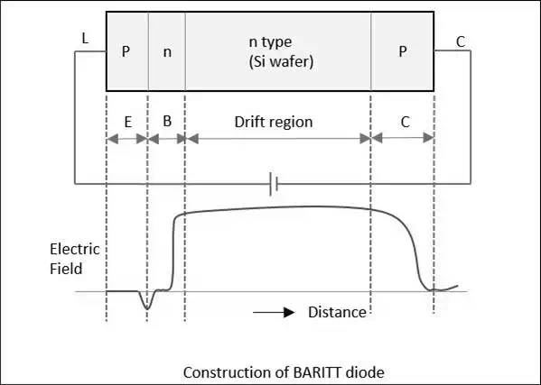
For a m-n-m BARITT diode, Ps-Si Schottky barrier contacts metals with n-type Si wafer in between. A rapid increase in current with applied voltage (above 30v) is due to the thermionic hole injection into the semiconductor.
The critical voltage (Vc)(Vc) depends on the doping constant (N)(N), length of the semiconductor (L)(L) and the semiconductor dielectric permittivity (ϵS)(ϵS)represented as




Comments are closed.