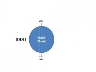
Complementary MOSFET (CMOS) technology is widely used today to form circuits in numerous and varied applications. Today’s computers, CPUs and cell phones make use of CMOS due to several key advantages. CMOS offers low power dissipation, relatively high speed, high noise margins in both states, and will operate over a wide range of source and input voltages (provided the source voltage is fixed)
For the processes we will discuss, the type of transistor available is the Metal-Oxide-Semiconductor Field Effect Transistor (MOSFET). These transistors are formed as a ‘sandwich’ consisting of a semiconductor layer, usually a slice, or wafer, from a single crystal of silicon; a layer of silicon dioxide (the oxide) and a layer of metal.
Structure of a MOSFET

As shown in the figure, MOS structure contains three layers −
![]() The Metal Gate Electrode
The Metal Gate Electrode
![]() The Insulating Oxide Layer (SiO2)
The Insulating Oxide Layer (SiO2)
![]() P – type Semiconductor (Substrate)
P – type Semiconductor (Substrate)
MOS structure forms a capacitor, with gate and substrate are as two plates and oxide layer as the dielectric material. The thickness of dielectric material (SiO2) is usually between 10 nm and 50 nm. Carrier concentration and distribution within the substrate can be manipulated by external voltage applied to gate and substrate terminal. Now, to understand the structure of MOS, first consider the basic electric properties of P – Type semiconductor substrate.
Concentration of carrier in semiconductor material is always following the Mass Action Law. Mass Action Law is given by −
Where,
v n is carrier concentration of electrons
v p is carrier concentration of holes
v ni is intrinsic carrier concentration of Silicon
Now assume that substrate is equally doped with acceptor (Boron) concentration NA. So, electron and hole concentration in p–type substrate is
Here, doping concentration NA is (1015 to 1016 cm−3) greater than intrinsic concentration ni. Now, to understand the MOS structure, consider the energy level diagram of p–type silicon substrate.

As shown in the figure, the band gap between conduction band and valance band is 1.1eV. Here, Fermi potential ΦF is the difference between intrinsic Fermi level (Ei) and Fermi level (EFP).
Where Fermi level EF depends on the doping concentration. Fermi potential ΦF is the difference between intrinsic Fermi level (Ei) and Fermi level (EFP).
Mathematically,
The potential difference between conduction band and free space is called electron affinity and is denoted by qx.
So, energy required for an electron to move from Fermi level to free space is called work function (qΦS) and it is given by
The following figure shows the energy band diagram of components that make up the MOS.

As shown in the above figure, insulating SiO2 layer has large energy band gap of 8eV and work function is 0.95 eV. Metal gate has work function of 4.1eV. Here, the work functions are different so it will create voltage drop across the MOS system. The figure given below shows the combined energy band diagram of MOS system.

As shown in this figure, the fermi potential level of metal gate and semiconductor (Si) are at same potential. Fermi potential at surface is called surface potential ΦS and it is smaller than Fermi potential ΦF in magnitude.
Working of a MOSFET
MOSFET consists of a MOS capacitor with two p-n junctions placed closed to the channel region and this region is controlled by gate voltage. To make both the p-n junction reverse biased, substrate potential is kept lower than the other three terminals potential.
If the gate voltage will be increased beyond the threshold voltage (VGS>VTO), inversion layer will be established on the surface and n – type channel will be formed between the source and drain. This n – type channel will carry the drain current according to the VDS value.
For different value of VDS, MOSFET can be operated in different regions as explained below.