INTRODUCTION
The entire CAD process that is necessary to implement a circuit in an FPGA (from the RTL description of the design) consists of the following steps:
• Logic optimization. Performs two-level or multi-level minimization of the Boolean equations to optimize area, delay, or a combination of both.
• Technology mapping. Transforms the Boolean equations into a circuit of FPGA logic blocks. This step also optimizes the total number of logic blocks required (area optimization) or the number of logic blocks in time-critical paths (delay optimization).
• Placement. Selects the specific location for each logic block in the FPGA, while trying to minimize the total length of interconnect required.
• Routing. Connects the available FPGA’s routing resources1 with the logic blocks distributed inside the FPGA by the placement tool, carrying signals from where they are generated to where they are used. Routing is an important step of the process as most of the FPGA’s area is devoted to the interconnect [21], and the interconnection delays are greater than the logic delays of the designed circuit. Therefore an efficient routing algorithm tries to reduce the total wiring area and the lengths of critical-path nets to improve the performance of the circuit; and for this, the router needs the interconnect information of the target FPGA architecture. This means that the problem of routing is architecture dependent and therefore the number of routers needed to route FGPAs is as varied as FPGA architectures there are in the market.
To understand better this dependency between routing and the target architecture, an overview of one of the most important commercially available FPGAs is shown below
• Xilinx
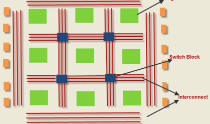
The general architecture of Xilinx FPGAs consists of a two-dimensional array of programmable blocks, called Configurable Logic Blocks – CLBs [24], with horizontal and vertical routing channels between CLB’s rows and columns. The routing resources available on this architecture are:
A. Connection boxes
The C boxes connect the channel wires with the input and output pins of the CLBs. It has two major properties that can affect the routability of a design: its flexibility, Fc, which is the number of wires that each logic block pin can connect to; and its topology, which is the pattern of switches2 that make the connection (especially if Fc is low). For example in figure 1, for a C box with Fc = 2, topology 1 can not connect pin A with pin B, meanwhile topology 2 can.

B. Switch boxes:
The S boxes allow wires to switch between vertical and horizontal wires. Its flexibility, Fs, defines for a wiring segment entering the S block the number of other wiring segments it can be connected to. The topology of the S blocks is very important since it is possible to choose two different topologies with the same flexibility Fs that result in very different routabilities. For example, figure 2 shows that meanwhile topology 1 can’t connect wire A with B, topology 2 can.

Fig. 2. Switch box topology Switch boxes that connect only tracks in the same domain, i.e. 0-0, 1-1, are called planar or subset switch boxes. Switch boxes that allow connection to any other domains, i.e. 0-3, 1-2, are called Wilton switch boxes, and they are broadly used as they provide greater flexibility on routing.
C. Single-length lines.
They are intended for relatively short connections among CLBs and they span through one CLB only. See figure 3.b.
D. Double-length lines.
They are similar to the Single-length Lines, except that each one spans two CLBs, offering lower routing delays for moderately long connection.
E. Long lines
They are appropriate for connections that require reaching several CLBs with low-skew. See figure 3.c.


Increasing the flexibility of the switch box, the connection box and the number of wires per channel makes routing a trivial problem [17] as all possible interconnections are available. But increasing routing resources has the drawback that waste area and transistors in the FPGA, as only a fraction of those resources will be used for a given design, even worse it increases the number of interconnect transistors which are the principal reason of delay on FPGAs. As FPGAs have prefabricated routing resources, the router must work within the framework of the architecture’s resources, deciding exactly which routing resources will be used to carry the signals between ELECTRÓNICA – UNMSM Nº17, Agosto del 2006 25 logic blocks, and making sure that no more connections are made through a region than there are resources to support them. Thus the router must consider the congestion of signals in a channel, and through multiple iterations rip out and reroute those congested areas and wires. This search of possible connections to route the placed logic blocks is not ensured to be feasible and it is possible that after a given number of iterations, 40 for example, the circuit can’t still be routed and the placement has to be redone. Therefore, together with the routing algorithm a routability detection algorithm is clearly desirable to avoid long routing iterations on designs that eventually will be determined to be unroutable.


Comments are closed.