Not so long ago, most software was permanently shipped along with their respective hardware, and there was no way to change it. But as technology matured, manufacturers found ways to update the software with additional features on existing hardware.
Now, imagine a future where hardware updates also become a possibility — wouldn’t that be fascinating?
Well, such programmable hardware whose sub-system configurations can be modified even after fabrication, falls under the category of Reconfigurable System. And the most predominant integrated circuit that supports reconfigurable computing is FPGA, an acronym for Field Programmable Gate Array.
FPGA enables you to program product features, adapt to new standards, and reconfigure hardware for specific applications even after the product has been installed in the field — hence the term ‘field-programmable’. Whereas ‘gate arrays’ refer to two-dimensional array of logic gates present in its architecture.
All modern personal computers including desktops, notebooks, smartphones, and tablets, are examples of general-purpose computers. General-purpose computing incorporates ‘Von Neumann’ approach, which states that an instruction fetch and a data operation cannot occur simultaneously. Therefore, being sequential machines, their performance is also limited.
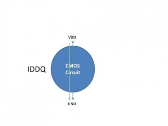
On the other hand, we have the Application Specific Integrated Circuits (ASICs) which are customized for a particular task like a digital voice recorder or a high-efficiency Bitcoin miner. An ASIC uses a spatial approach to implement only one application and provides maximum performance. However, it can’t be used for the tasks other than those for which it has been originally designed.
So, how about trading off the performance of ASICs for the flexibility of general-purpose processors?
Well…
FPGAs act as a middle ground between these two architectural paradigms!
Having said that, FPGAs are less energy efficient when compared to ASICs and also not suitable for large volume productions. However, they are reprogrammable and have low NRE costs when compared to an ASIC.
You see, ASICs and FPGAs have different value propositions. Most device manufacturers typically prefer FPGAs for prototyping and ASICs for very large production volumes.
FPGAs used to be chosen for lower speed and complex designs in the past, but nowadays FPGAs can easily surpass the 500 MHz performance benchmark.
Internal Architecture of FPGA
In 1985, a semiconductor manufacturing company named Xilinx invented the first commercially viable FPGA — XC2064. Another company Altera, which was acquired by Intel in 2015, also pushed the boundaries and drove this market forward along with Xilinx.
FPGA emerged from relatively simpler technologies such as programmable read-only memory (PROM) and programmable logic devices (PLDs) like PAL, PLA, or Complex PLD (CPLD).
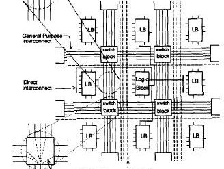
It consists of three main parts:
· Configurable Logic Blocks — which implement logic functions.
· Programmable Interconnects — which implement routing.
· Programmable I/O Blocks — which connect with external components.

Logic blocks implement the logical functions required by the design and consist of various components such as transistor pairs, look-up tables (LUTs), flip flops, and multiplexers.
You can think of logic blocks as separate modules like lego blocks which can operate in parallel. Unlike a lego block, a logic block is configurable i.e. its internal state can be controlled and you can hook these together by programming the interconnects in order to build something meaningful.
This hierarchy of programmable interconnection is used for allocating resources among configurable logic blocks (CLBs); where routing paths contain wire segments of varying lengths that can be connected via anti-fuse or memory-based techniques.
Each CLB is tied to a switch matrix to access the general routing structure. The switch matrix provides programmable multiplexers, which are used to select the signals in a given routing channel and thereby connect vertical and horizontal lines.
Lastly, the I/O blocks (IOBs) are used to interface the CLBs and routing architecture to the external components.
In earlier FPGAs, there was no processor to run any software; hence implementing an application implied designing the circuit from scratch. So, we could have configured an FPGA to be as simple as an OR gate or as complex as the multi-core processor.
But we have come a long way since XC2064 and the basic FPGA architecture has developed through the addition of more specialized programmable function blocks like ALUs, block RAM, multiplexers, DSP-48, and microprocessors.


Comments are closed.