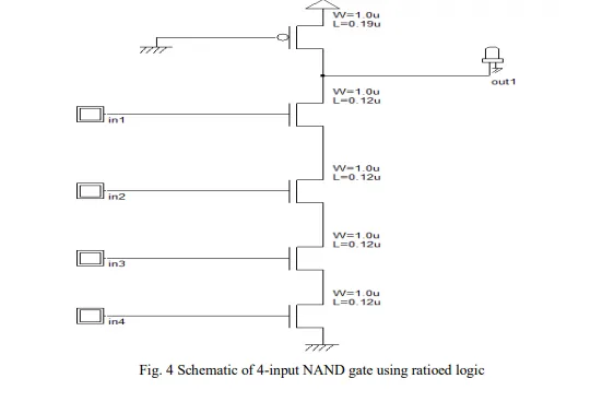
Ratioed MOS circuits have been known for many years, and were used widely in the past despite their high power dissipation because they are fast static circuits[3]. Ratioed circuits use weak pull-up devices and stronger pull-down devices. They reduce the input capacitance and hence improve logical effort by eliminating large PMOS transistors loading the inputs. Fig.4 shows the schematic circuit diagram of 4-input NAND gate using pseudo-NMOS logic gates, which are the most common form of CMOS ratioed logic. The pull-down network is like that of a static gate,but the pull-up network has been replaced with a single pMOS transistor that is grounded so it is always ON[1]. The main advantage of 4 -input pseudo NMOS logic gate is that there is 1-pMOS and 4-NMOS transistors is used, so the number of components has reduced and area also reduced. It also reduces the complexities of the circuit. Because of less hardware used so the capacitance become reduced
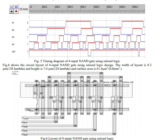
In fig.5 shows the timing operation performed on 4-input NAND gate using ratioed logic design, the rise delay and fall delay calculated is 0.005 ns and 0.001ns respectively.
