• N transistors
• No static consumption
Primary inputs drive the gate terminals + source-drain terminals. In contrast to static CMOS – primary inputs drive gate terminals.
Example: AND Gate
When B is “1”, top device turns on and copies the input A to output F. When B is low, bottom device turns on and passes a “0”. The presence of the switch driven by B is essential to ensure that the gate is static – a low-impedance path must exist to supply rails. Adv.: Fewer devices to implement some functions. Example: AND2 requires 4 devices (including inverter to invert B) vs. 6 for complementary CMOS (lower total capacitance). NMOS is effective at passing a 0, but poor at pulling a node to Vdd. When the pass transistor a node high, the output only charges up to Vdd-Vtn. This becomes worse due to the body effect. The node will be charged up to Vdd – Vtn (Vs )


NMOS-Only Logic

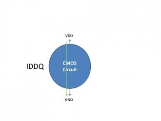
Energy Consumption

Complementary Pass Transistor Logic

Since circuit is differential, complimentary inputs and outputs are available. Although generating differential signals require extra circuitry, complex gates such as XORs, MUXs and adders can be realized efficiently.
• CPL is a static gate, because outputs are connected to Vdd or GND through a low-resistance path (high noise resilience).
• Design is modular – all gates use same topology; only inputs are permuted. This facilitates the design of a library of gates.